HI-FI audio fanatics 616Wrms bridge amplifier
1. OVERVIEW
It is a high fidelity powerful and reliable amplifier designed for audio fanatics and professionals.
It can deliver 208Wrms on 1.7ohm load at +/-32Vdc and 308Wrms on 1.7ohm at +/-40Vdc.
I built it bridgeable so bridging two EnhancedAmps, 616Wrms can be delivered on 3.4ohm load at +/-40Vdc !
On board is also a clip detector who drives a front panel mounted clip LED.
Built around the DMOS technology TDA7293 this amplifier sounds amazing, like a tube amplifier, making the music sound better, smoother, warmer and cleaner.
2. GENESIS
It came as a development of the schematic proposed by Dr. Frost on dyiAudio
(http://www.diyaudio.com/forums/chip-amps/206591-tda7294-power-transistors-amp-tda7293-come-also.html).
I published first schematic of this amplifier on June 15, 2015 on same forum and added comprehensive measurments on July 1, 2015 ( http://www.diyaudio.com/forums/chip-amps/206591-tda7294-power-transistors-amp-tda7293-come-also-50.html).
On April 2016 diyAudio member #buciflex contacted me for assistance because he was willing to do the work to build a PCB for the Enhanced amp. We decided to add on board the clip detector and provision for bridge connection.
#buciflex found out the best component placement and I routed the PCB in the actual form.
More theory about this amplifier and test results HERE.

3. SCHEMATIC
The electronic schematic of the EnhancedAmp is:

J1 is the power connector. +Vdc, -Vdc, GND. V range is from +/-12Vdc to +/-45Vdc. Both +V and -V are fuse protected on board.
J2 is the input signal connector.
J3 is the speaker connector. Any impedance speakers in range of 1.5 - 16 ohms can be used.
J4 is the clip detector output. A LED can be connected to this output and placed on the front panel of the amplifier to show if clipping appears in order to reduce input signal to avoid distortions.
J5 is the bridge connector. Bridging means to have 2 EnhancedAmps, one as master and the other as slave. The master inputs the audio signal for the bridged amplifier, the slave input must be shorted. Pin 2 of master BRIDGE connector must be tied to pin 1 of the slave BRIDGE connector. The speaker will not be connected to ground but between pins 2 of OUT connectors of the two amplifiers.
Bridge configuration quadruples the output power on same load but the current supported by the amplifier is double. So the range of allowed speakers impedances doubles also, starting from 3 ohm instead of 1.5 ohm. Is ok to bridge two EnhancedAmps who deliver 154Wrms on 3.4 ohm load each at +/-40Vdc. The bridged amplifier will deliver 154 x 4 = 616Wrms on same 3.4 ohm load. In this example the equivalent single amplifier load for each will be 1.7 ohm.
J6 was introduced in schematic for the PCB design program to separate the traces of analog ground and power ground. On PCB this jumper must be shorted.
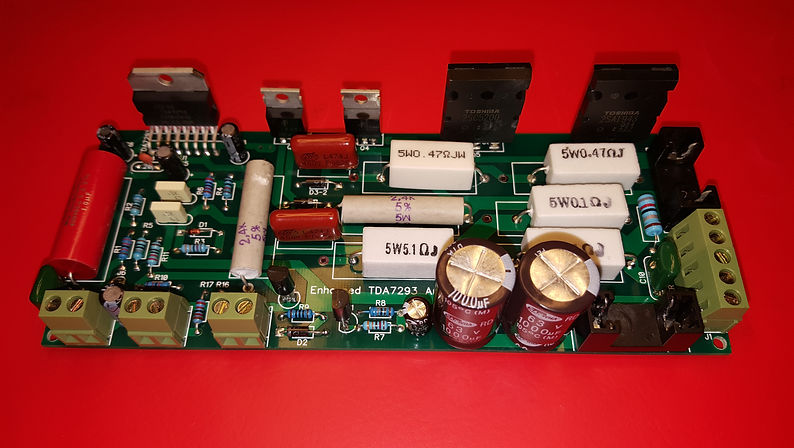
4. PCB
The PCB dimensions are 162 x 64mm. The size of the board was imposed by the necesity to dissipate the heat produced by TDA, power transistors and power resistors.

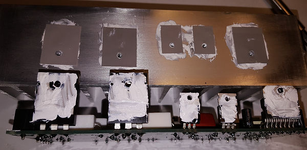
The power active components are placed on the top edge of the board to be attached on a unique heat sink.
The space between this components is according to the heat produced by each of them to allow the heat sink to better absorb heat.
The dimension of the heat sink is related to the power delivered on speakers and for more than 100Wrms I recommend that the heat sink to be vented by a fan.
Power passive components populate the right side of the board and are spaced enough to dissipate the heat.
On the right side are placed also the speaker and power connectors. Note that this amplifier requires a separate rectifier-filter circuit, with at least 20000uF capacitors for each voltage polarity.
The fuses are also convenient placed on the edges of the board being easy accessible.
On the bottom left of the board, far from power signals are placed the small signal connectors, the audio input and the BRIDGE connector.
The CLIP connector is also on the bottom of the board.
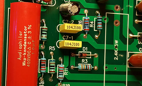
Audio input signal comes across an audiophile quality capacitor having a good response across the entire audio band of frequencies.
5. EQUIPPED BOARD

6. COMPONENTS

7. ASSEMBLY INSTRUCTIONS
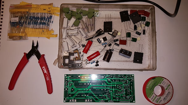

Carefully select the 3pcs 22Kohm resistors and the 2pcs 680 ohm to be as close to the designated values as possible.
1. First solder the 0.25W resistors. Following the schematic you find for every resistor the value and the reference number as R6 for example. This reference numbers are written on the PCB so you can easily find every component's place.
2. Solder the diodes taking care of their orientation. The line who marks the cathode end on the diode itself must match the line of the diode depicted on PCB.
3. Solder the 8.2 ohm/1W resistor
4. Solder the small polarized capacitors, 2 x 10uF, 1 x 22uF and 2 x 47uF. Be careful of their polarity. On PCB the + pin is marked, on capacitors usually the - pin is marked. For C5 and C6 respect their voltage!

5. Solder C4 the 120pF ceramic capacitor, then the two 0.1uF decoupling capacitors C7-1 and C7-2
6. Solder the 5W resistors and the 1uF input capacitor
7. Solder the fuse holders and the connectors

8. Solder C2-1 and C10 o.1uF capacitors
9. Solder Q1 and Q2 2SA1013 transistors
10. Solder C9-1 and C9-2 470uF capacitors
11. Solder Q3 and Q4. Be careful to place MJE15030 (TIP41C) on Q3 mark and MJE15031 (TIP42C) on Q4 mark.
The terminals of this transistors must be fully inserted into PCB. When soldering the terminals hold them in vertical position versus PCB.
12. Solder Q5 and Q6. Q5 = 2SC5200, Q6 = 2SA1943. The terminals of this transistors must be fully inserted into PCB. When soldering the terminals hold them in vertical position versus PCB.

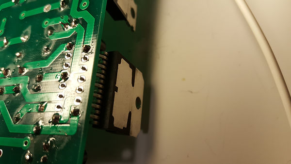
13. Soldering TDA7293 requires much more attention than the rest of components. If you disregard any of this instruction you may end up with a broken TDA7293 after soldering!
- Set the temperature of soldering iron to 250 degrees Celsius no more!
- Attach a wire to the PCB ground (POWER connector middle) and connect it to the mains protection ground
- Be sure that the soldering iron is also by construction connected to the mains protection ground, if not connect it!
- Connect yourself to the mains protection ground with a bracelet or a uninsulated wire wrapped around your wrist and connected to mains protection ground
- Now you can insert the TDA7293 into PCB with terminals exiting about 0.5mm on the back side of PCB. TDA must be vertical.
- Solder pins one by one in random order avoiding to solder adjacent pins one after the other.

14. Solder the 1000uF/63V capacitors being careful to respect the polarity.
15. From a capacitor or diode terminal make a U-shape and shorten J6 connector, soldering on the back.


Don't insert yet the fuses in holders.
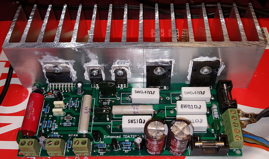
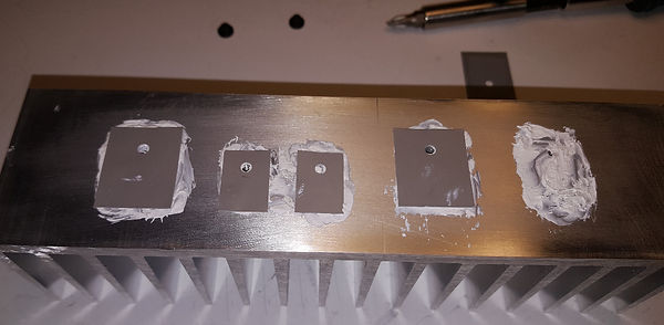
8. ATTACHING THE HEAT SINK
Heat sink is as important as the power supply is. In order to deliver power, TDA7293 and transistors need to properly dissipate heat to maintain them under the limit temperature. Failure to cool enough these components may lead to permanent damage them. As much power we demand from the amplifier as big the heat sink must be. In practice above a certain power the radiator must be vented by fan.
The radiator I used in this tutorial is 200mm x 100mm and fins are 50mm deep.
It can be used up to 100Wrms delivered in speakers without fan, but the fins must be uncovered and in open air to assure natural ventilation. Don't insert heat sinks completely inside the amplifier case unless it is ventilated by fan(s)!
For 300Wrms I suggest an 200mm x 150mm of same kind of radiator (taller) and a 100mm x 100mm 12V computer fan attached to the fins.
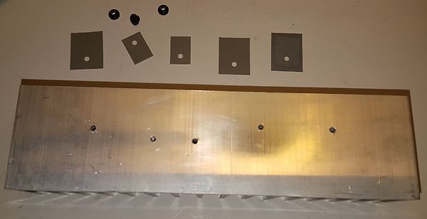

Mark center of holes of power components and drill using 2.5mm bit.
Bottom of PCB must be 5mm above the bottom of heat sink. Drill holes deep enough to accomodate full length of screws.
Turn the 3mm diameter screws in to format the threads.
Remove the screws. Notice the unfinished margin of holes that might break the insulating pads.
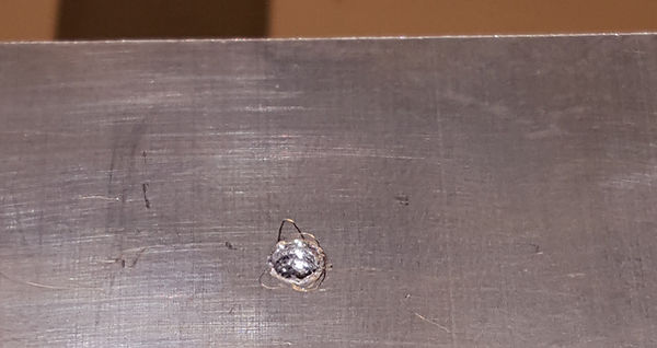
Smooth finish using soft sandpaper then clean heat sink using isopropylic alcohool.
Use heat sink compound to stick insulating pads to heat sink.
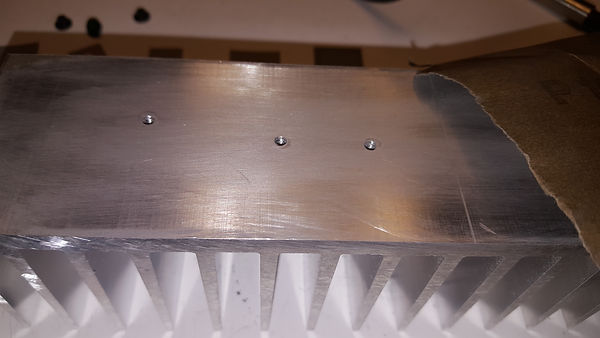
Pour heat sink compound on metal side of power components.
Insert screws in power components attaching holes using insulating sleeves for metal ones. Don't tighten a screw at once, insert screws step by step, few turns each to even approach the components to heat sink.
Firmly tighten the screws to assure good heat transfer. Using an ohmmeter check that radiator is insulated of every metal part of power components.


8. START UP
Never connect the amplifier to power without attaching the heat sink!
All the power components must be insulated from the heat sink using silicone insulators. Use plastic sleeves around the attaching screws of TDA and TIP transistors. Also plenty of silicone thermal conducting compound must be used on both sides of silicone pads.
If possible, it is advisable to check the board, powering it first from +/-12Vdc lab power supply with current limit. If not available, do this test using your final power supply. Set the current limit of lab power supply to 200mA for both voltages. Connect the power supply wires to amplifiers POWER connector. Power on the power supply(es) and check the polarity at POWER connector with a voltmeter. The connector terminal over the GND terminal must be negative and the one under GND must be positive.
Switch off the power supply and insert the fuses in holders. Short the IN connector. Power on again. If two different power supplies are used start FIRST and switch off last the negative voltage supply. NEVER power only positive voltage, nor positive voltage first!
Check the current absorbed. It must be between 50mA to 120mA on both polarities for +/-12Vdc and up to 200mA for +/-40Vdc.
Measure the voltage on speaker connector. It must be close to 0Vdc, no more than 80mVdc.
Now power off, connect the preamp and speaker(s) and enjoy!
9. POWER SUPPLY
Some considerations must be taken care of in building a power supply for this amplifier.
The working voltage range admitted by this amplifier is from +/-12Vdc to +/-45Vdc. Make your computation and be sure that in any circumstances the power supply won't reach +/-50V or over!
Choose a transformer having the VA power 150% greater than the RMS power desired on speakers.
For example for the 308Wrms on 1.7ohm at +/- 40Vdc a 308 x 1,5 = 462VA transformer is requested. Round the value to the closest available transformer. A 450VA transformer will do the job.
A simplified mode to find out the transformers secondary voltage is computing (+Vdc+2)/sqrt(2). For the above example (40+2)/sqrt(2)=29.69Vac. A 450VA transformer with two 30Vac windings will be fine. However under heavy load the rectified voltage drops by 4-6Vdc. To be sure you will get the designed power of 308W without clipping, redo the computation adding 5V. Now the requested +/- voltage will be 40V+5V = 45V. (45+2)/sqrt(2)=33.23Vac. So the best transformer for this example will be a 450VA transformer with 2 windings delivering 33Vac each. Anyway I don't recommend to go over this value of 33Vac because, due to mains power supply fluctuations, it will be easy to cross the 50V maximum limit.
The capacity of the filtering capacitors is also very important. As a thumb rule consider 10000uF for every 100Wrms on speakers, for each power supply polarity. For the example above, 6 capacitors of 10000uF must be used, 3 on the +V and 3 on -V.